Feb 01, 2024
Operational Amplifier Design & Calculations
Introduction
This post covers the design and calculations for a simple 2-stage operational amplifier.
The design uses a simple OTA as the first stage and a common-source amplifier for the output stage. Cascode transistors are used to improve accuracy and overall gain of the amplifier. Compensation is implemented to increase the system phase margin and to improve stability at high frequency.
Limitations: these are my personal notes which cover the bulk of initial designs; they are not meant as outline for a complete design process.
Design Specification
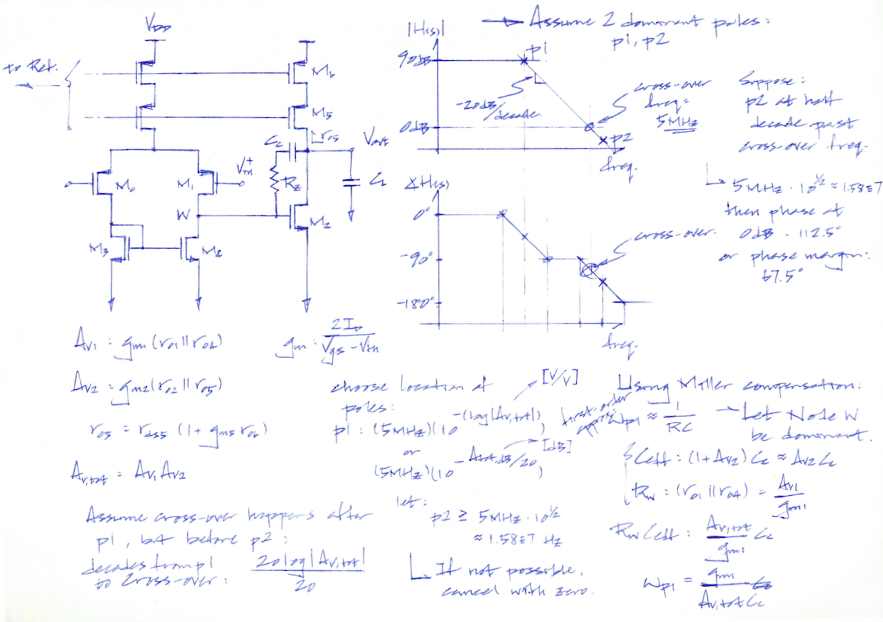
- P-MOS input, N-MOS output
- DC gain > 90dB
- UGW = 5MHz
- PM: ~60$^\circ$
Calculations
This section discusses the calculations used in the example circuit (illustrated in the above schematic/sketch).
DC Gain $A_{V,tot}$
 Determining the expression for total DC gain is straight-forward. When the amplifier is simplified into the above functional stages, we see that
$$
A_{V,tot} = A_{V1}A_{V2}
$$
Determining the expression for total DC gain is straight-forward. When the amplifier is simplified into the above functional stages, we see that
$$
A_{V,tot} = A_{V1}A_{V2}
$$
Since the two stages are both effectively common-source amplifiers, their gain take on the form $A_V = g_m r_o$.
Referencing the designators in the schematic, we can write the expressions as
$$ \begin{align} A_{V1} &= g_{m1}(r_{o1} || r_{o4}) \tag{$\ast$}\label{Av1} \\ A_{V2} &= g_{m2}(r_{o2} || r_{o5}), \quad r_{o5} = r_{ds5}(1+g_{m5}r_{o6}) \tag{} \end{align} $$
During initial design, the $g_m$ values can be coarsely approximated using the expression
$$ g_m = \frac{2I_D}{V_{gs}-V_{th}} $$
In practice, we should determine the values by first characterizing and plotting $g_m/I_D$ curves of the transistors. To pick the values for $A_{V1}$ and $A_{V2}$, we need to take into account the total system's frequency response.
Placing $p_1$ and $p_2$
Recall that the design requirements specify a unity gain frequency (UGW) of 5MHz. We can assume that the system has two dominant poles $p_1$ and $p_2$ (at $\omega_{p1}$ and $\omega_{p2}$, respectively). We further assert that $p_2$ is at a frequency higher than UGW and that it does not participate significantly in the initial roll-off — the justification for this assertion is that we require it to be the case, since having two poles before cross-over leads to instability of the overall system.
Using these conditions, we determine the location of $p_1$ by drawing a line at a slope of $-20\text{ dB}/\text{decade}$ from $(5\text{ MHz},0\text{ dB})$ to where it intersects a horizontal line at 90dB (the DC gain of the system).
Idealized Bode plots of system transfer function $H(s)$
Mathematically, this is can be computed as
$$ \begin{align*} p_1 &: (5\text{ MHz})(10^{-\operatorname{log|A_{V,tot}|}}),\quad A_{V,tot}:\text{ [V/V]} \\ &= (5\text{ MHz})(10^{- A_{tot,dB} / 20}),\quad A_{tot,dB} = 90\text{ [dB]} \\ &= (5\text{ MHz})(10^{-4.5}) \\ &= \boxed{158\text{ Hz}} \end{align*} $$
Thus, we choose to place $p_1$ at $\omega_{p1} = 158\text{Hz}$
As for the location of $p_2$, it is convenient to approximate its location with an idealized Bode phase plot, in which a pole contributes -90$^\circ$ total phase change, beginning 1 decade before the pole frequency and finishing 1 decade after. Suppose $p_2$ is placed half a decade after cross-over, it will contribute -22.5$^\circ$ of phase shift to the system response at the cross-over frequency. In other words, the total phase shift at cross-over will be -112.5$^\circ$ (-90$^\circ$ from $p_1$ + -22.5$^\circ$ from $p_2$), giving the system a phase margin of 67.5$^\circ$ (-180$^\circ$ - -112.5$^\circ$ = 67.5$^\circ$) — close to the target phase margin of 60$^\circ$.
$$ \text{Choose }p_2: (5\text{ MHz})(10^{1/2}) = \boxed{1.58\times 10^{7} \text{ Hz}} $$ In practice, this placement is difficult to achieve without compensation, so we typically employ Miller compensation technique to simulatneously shift (split) the pole locations and introduce additional phase margin by injecting a zero in between.
Compensation
System stability is improved when we leverage Miller effect and introduce a zero between the poles. When compensator capacitor $C_C$ is placed between the input and output nodes of the second stage amplifier, its effective input capacitance is
$$ C_{eff} = (1+A_{V2})C_C \approx A_{V2}C_C $$
The approximation assumes a large stage 2 gain $A_{V2}$, as is typical (and practical) for such topology, and a small value for $R_z$ — typically only a few ohms. As such we also assume the node between stage 1 and stage 2, node W, to be responsible for dominant pole $p_1$. This assumption allows us to then make the approximation
$$ \omega_{p1} \approx \frac{1}{R_W C_{eff}}, \quad \text{where } R_{W} = (r_{o1}||r_{o4}) = \frac{A_{V1}}{g_{m1}} $$
Conveniently, $R_W$ is simply a rewriting of the $A_{V1}$ equation \eqref{Av1}. Putting the expressions together yields
$$ R_W C_{eff} \approx \frac{A_{V1}}{g_{m1}} \cdot A_{V2}C_C = \frac{A_{V,tot}C_C}{g_{m1}} $$
and
$$ \omega_{p1} \approx \frac{g_{m1}}{A_{V,tot}C_C} $$Finally, we derive the placement of the zero by making the observation that at $s_z$
$$ \left| \frac{V_{out}(s_z)}{V_W} \right| = 0 $$
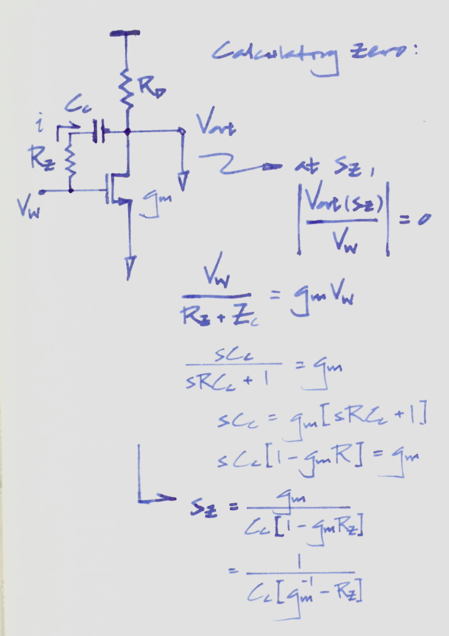
Approximating location of zero
Assuming load resistance is large (necessary to achieve high gain for $A_{V2}$), nodal analysis yields
$$ \begin{align*} \frac{V_W}{R_z + Z_c} &= g_m V_W \\ \frac{sC_C}{sR_z C_C + 1} &= g_m \\ \\ sC_C &= g_m [sR_z C_C + 1] \\ \\ sC_C[1-g_m R_z] &= g_m \end{align*} $$
We thus choose the initial value of $R_z$ using the following equation, with the condition that $\omega_{z} < \omega_{p2}$ $$ \omega_z = \frac{g_{m2}}{C_C [1-g_{m2} R_z]} $$
Remaining Steps
The above calculations can typically bring the design to about 80%~90% completion. The remaining steps of the design are to simulate the circuit under various process, voltage, and temperature conditions (typically at their extremes) and to run Monte Carlo simulations to assess noise. These final steps are instrumental in finalizing the dimensions of the devices as well as assuring performance of the circuit at all PVT extremes.