Jun 27, 2024
Design of Spread Spectrum Clock
Power spectral density: system clock with spread spectrum vs. no spread
Introduction
In this project, I design a Spread Spectrum Clock modulator in order to reduce the EMI emissions of an IC around the AM radio band. The entire design is done in Cadence Virutoso. Results are shown in the end.
Spread Spectrum Clocking (SSC) is a technique that helps reduce the radiated emissions of digital systems by modulating and shifting the frequency of clock signals. Due to the periodicity of the digital clock signals, electromagnetic interference (EMI) tends to concentrate about system clock frequencies as well as their odd harmonics. By slightly varying a system's clock freuquency, the overall emission is spread over a broader frequency range, reducing peak EMI and helping systems meet regulatory standards.
Design Specifications
In this design, I target high-frequency noise reduction in the AM band. The spread spectrum block modulates the input clock by ±5%, ±10%, ±15%, or ±20%, selectable by the user, and outputs the modulated clock. The input clock (central frequency) may be 384kHz, 480kHz, 576kHz, or 768kHz. The spread spectrum block has access to the master on-chip current reference (2µA).
Additionally, the system must maintain close adherance to a 50% duty cycle.
Software & Simulation Tools
The system is designed and simulated with Cadence Virtuoso.
System Overview
The functional design of this block is based on the circuit presented by Nagari et al.[1] (see figure below). We can see in this circuit that the master clock is first injected from the left side, and through a sequence of delays, the clock is systematically time-shifted to produce an output clock with varied frequency from one period to the next. Each delay block is structurally similar, with pass-through (no delay) as the top path and delayed signal as the bottom path. Path selection is done via the sequencer.
Delay Cell
The delay cell is the principle building block about which the rest of the system is designed. Its functional diagram is illustrated here.

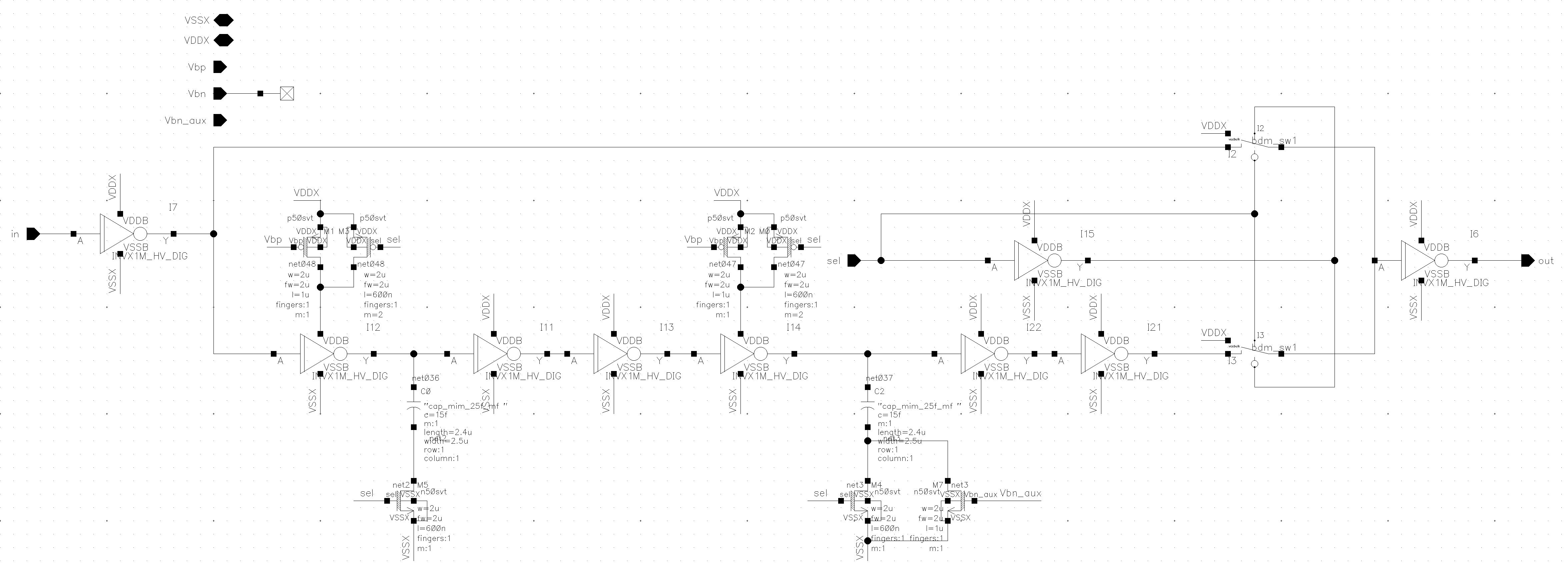
My rendition of spread spectrum clock is shown in here. Looking at the schematic, we can see that the master clock first enters from the left side, and is modulated by blocks Fine trim DL and Coarse trim DL. Fine trim DL and Coarse trim DL are functionally similar in that both impose ’jitters’ in frequency relative to the central (input) frequency — one smaller and the other larger in magnitude, respectively. Thus, for the purpose of discussion, we can simply choose one of the two blocks to examine.
DLSS system view
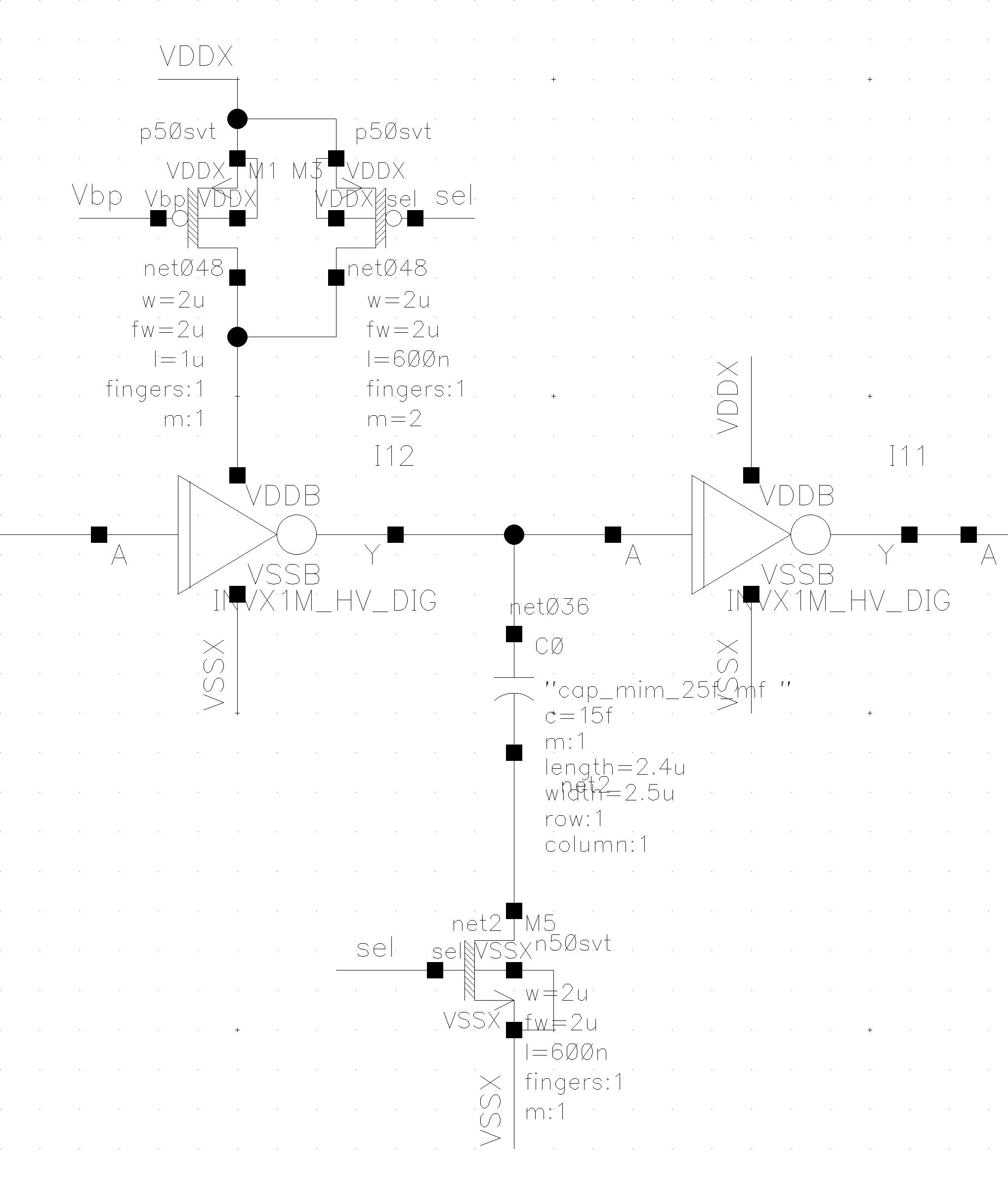
Figure 4 shows the internal structure of Coarse trim DL. The block is composed of multiple delay blocks. The delay blocks come in pairs (e.g. MUX delay cell 10n is repeated), as the first cell is responsible for delay of the first half period and the second cell effectively helps double the delay in the latter half period. Together, they ensure that the modulated clock maintains a duty cycle of 50%. See Figure 2 for visualization.
One of the details relating to correct output of the spread spectrum clock is the fact that the delay cells are designed to apply asymmetric delays to the rising and falling edges of the incoming clock signal. This is because applying the same delay to both results in overall unequal $t_{on}$ and $t_{off}$.
Looking at the DLSS schematic (Figure 3), we can see that the master clock first enters from the left side, and is modulated by blocks Fine trim DL and Coarse trim DL. Fine trim DL and Coarse trim DL are functionally similar in that both impose ’jitters’ in frequency relative to the central (input) frequency — one smaller and the other larger in magnitude, respectively. Thus, for the purpose of discussion, we can simply choose one of the two blocks to examine. Figure 4 shows the internal structure of Coarse trim DL. The block is composed of multiple delay blocks. The delay blocks come in pairs (e.g. MUX delay cell 10n is repeated), as the first cell is responsible for delay of the first half period and the second cell effectively helps double the delay in the latter half period. Together, they ensure that the modulated clock maintains a duty cycle of 50%. See Figure 2 for visualization.

Delay block
Linear delay element
DLSS system view
Figure 4 shows the internal structure of Coarse trim DL. The block is composed of multiple delay blocks. The delay blocks come in pairs (e.g. MUX delay cell 10n is repeated), as the first cell is responsible for delay of the first half period and the second cell effectively helps double the delay in the latter half period. Together, they ensure that the modulated clock maintains a duty cycle of 50%. See Figure 2 for visualization. To achieve the activation sequence as seen in Figure 2, we utilize D flip-flops with inverted clock signals (CLK D & CLK Db) such that the second delay block is only activated on the falling edge of the input clock (relative to the delay pair). The delay pairs are enabled sequentially, with the sequence determined by input signal buses Fine trim<1:0> & Coarse trim<2:0>.
some math reference things, \(y=m x+ b\), math stuffs
$$ block math $$
const msg = "hello, world";
console.log(msg);
\begin{equation}\label{complex} e^{\pi i} + 1 = 0 \end{equation}
\begin{equation} E = mc^2 \label{eq:einstein} \end{equation}
refer to eqn \ref{eq:einstein}
123
Autonomous Tetris Agent
123
Fluid Dynamics Simulation in a Venturi Tube
123
Bipedal Compass-Gait Walker
123
Surface Referencing Against Deformable Soft Bodies
123
Operational Amplifier Design & Calculations
123
Design of Spread Spectrum Clock
123
Closing the Loop: Visual-Tactile Feedback for Robotic Grippers
123
Contact-Aware Pick and Place with a 6-DoF Arm
123
Post 0
123
Techniques in System Identification
References
- A. Nagari, E. Allier, F. Amiard, V. Binet and C. Fraisse, "An 8 Ω 2.5 W 1%-THD 104 dB(A)-Dynamic-Range Class-D Audio Amplifier With Ultra-Low EMI System and Current Sensing for Speaker Protection," in IEEE Journal of Solid-State Circuits, vol. 47, no. 12, pp. 3068-3080, Dec. 2012, doi: 10.1109/JSSC.2012.2225762.