
Homemade 3-Axis CNC Machine
Figure 1; Videos:

a) Z-axis Demo

b) MDF Milling Demo
Introduction
When I was 15yrs old, I spent about a year developing this budget CNC machine from scratch. At the time, consumer grade CNC machines, 3D printers, and their corresponding components were not yet commonly available. This meant that to build a machine of this size with good performances, all while keeping costs low, was a major challenge. Nevertheless, I was determined…
I designed this machine to be built from commonly available hardware store items. The overall structure of the machine is made of MDF — a dimensionally stable, vibration damping, and low-cost material — as well as standard ¼” - 20 threaded rods, and a Dremel rotary tool for the spindle.
For actuation of the machine, each axis is driven by a stepper motor via the ¼” - 20 threaded rods. And each motor is driven by custom-designed high power motor controllers. The stepper motors were found through a liquidation sale, which meant that they came with minimal information on their specification. These cheap motors later posed many challenges to the design of the motor controller and the motion control algorithm, which will be discussed in detail in this post.
The resulting system is exceptionally low-cost, but achieving this required overcoming many design hurdles.
Challenges
Almost all of the challenges arise from using less than optimal components for the drive trains. First, we have the ¼” - 20 threaded rods, which are suboptimal for driving linear motion. They are slow, requiring many revolutions from the actuating motor to move a given distance (Note that the ‘20’ denotes the number of revolutions per inch). In other words, it requires fast stepping from the stepper motors to move the machine effectively. In addition they also tend to be quite stiff to drive: to combat backlash, I used plastic nuts with very tight thread meshing along each axis, which in turn creates a lot of friction. The consequence of this is that the drive train requires moderately high driving torque (proportional to current) from the motors to avoid stalling.
Figure 2: major sources of challenges
The problem is further compounded by poor characteristics of the stepper motors. The motors have high inductances and low resistances which result in large characteristic time constants — slow actuation. At the same time, they are unable to handle large steady-state currents which aid in providing driving torque.
The result of all of this is that the custom driver circuits need to be high-powered and sophisticated with its timing and driving sequence to use the motors effectively.
System Overview
In this section, I will be introducing an overview of the system and discuss the scope of this post.
First, we will not be discussing the mechanical design of the system. Instead, we will only be examining the electrical portion of the system. Here is an overview diagram of the electrical system:
Figure 3: electrical system overview
Starting from the left, we have a PC, which takes 3D models/tool paths and convert the machine operations into G-Code via a G-Code sender. The G-Code sender sends the information by USB or parallel port interface to a hardware implemented G-Code translator, which is responsible for servicing user interfaces as well as distributing the drive signals to the motor controllers responsible for controlling each axis of the machine. Each axis of the machine is controlled by one MCU, two H-bridges, and a stepper motor. For this post, we will primarily be focusing on the portion of the system circled in red.
Problem
Let’s discuss our design problem.
I mentioned earlier that I acquired these mystery stepper motors with poor specifications. The problem was first identified when I performed a system identification on the motors. Using step inputs and observing the response from the motors, I was able to determine its characteristic parameters \(L_{0}\) and \(R_{0}\). Assume a first-order approximation, the system under test can be characterized by:
\[\tau_{test} = \frac{L_{0}}{R_{0}+R_{ext}}\], where \(R_{ext}\) is an external resistor connected in series with the motor winding and \(L_{0}\) and \(R_{0}\) are the characteristic inductance and resitance of the motor winding. By testing the system with different values of \(R_{ext}\), and measuring the motor current over time — to determine the corresponding time constant \(\tau_{ext}\) — we can calculate for \(L_{0}\) and \(R_{0}\). Using measurements shown in Figure 4, the values come out to:
\[\tau = {L_{0}}/{R_{0}} = 4.2 ms, \; L_{0}=1.61mH, \: R_{0}=0.387\Omega\], and we see that the characteristic time constant is very large!
a) \(\tau_{test} = 368 \mu s, \; R_{ext}=8.2 \Omega \)
b) \(\tau_{test} = 168 \mu s, \; R_{ext}=4 \Omega \)
Figure 4: identification of motor parameters through step response
In a broader scope, the large time constant means that it is difficult to actuate the motor windings quickly at low voltages. While high voltages correspond to faster actuation, they also lead to excessive winding currents at steady state; and the stepper motors are not designed to handle high steady-state currents.
With some napkin math, we figure out that — without any special circuitry — the machine is incredibly slow. Recall that each axis requires 20 revolutions to move one inch, and that the stepper motors take 200 steps to make one full rotation. In other words, each axis requires 4000 steps from a motor to move 1 inch. Assuming \(3\tau\) (corresponds to 95% of steady state current) for full actuation, it would take the machine more than 10min to move from one end to the other!
This is far too slow of a milling rate. As a general discussion of milling rate: feed rates that are too low, especially in the context of spindle runout (as is very much true for a Dremel rotary tool), tend to lead to burning of softer materials; and feed rates that are too high tend to cause chatter, breaking bits, and general bad dimensions.
Solution
It turns out, the solution is principally quite simple...
Consider the plot below of the motor winding current when actuated using different voltages (1.5V, 9V, 24V)
Figure 5: motor currents when driven with varied voltages
At the lowest actuation voltage, we have 1.5V, which is about the maximum permissible DC-voltage for driving these motors. The rise time to reach the desired target current is about 12.5ms.
Suppose for a second, we are allowed to use higher actuation voltages. With higher actuation voltages, the motor winding reaches the same target current at much faster rates. For the case of using 24V, the rise time is 0.25ms, or 50x faster.
By using a feedback loop and switching the applied voltage ON & OFF appropriately, we are actually allowed to use these higher voltages without generating excessive steady state dissipation on the motor windings. The name of this implementation is “Chopper drive”, which is a sort of constant-current based driver.
A simplified illustration of such a feedback loop is illustrated in Figure 6. At \(V_{S}\), the load is supplied a voltage much higher than what it permissible at steady state (e.g. 24V). A sense resistor on the “low-side” is used to measure the current flow through the load and a comparator detects when this current rises past a pre-set level. When triggered, the comparator cuts off the rising flow of current, thereby regulating the load and forming a current feedback loop.
Figure 6: simplified current-feedback loop [1]
Note that in real applications, special attention is made around ‘turn-off’ of the inductive load. Some example techniques for managing the current flow during ‘turn-off’ are listed below:
- "fast-decay"
- "slow-decay"
- Mixed, etc.
These methods will be discussed more in depth in the following sections.
Implementation
I will first discuss the basic implementation of the motor controllers, including the current-feedback loop. Afterwards, we will take a look at improvements which substantially improve the performance of the overall system.
The Basics
Figure 7: system diagram per axis
Above is a subsystem diagram for each axis. Recall that each motor or axis requires:
- 2 \(\times \) (H-bridge + H-bridge driver)
- 1 \(\times \) (MCU)
, and Figure 8 shows the bench testing setup for a prototype of this subsystem:
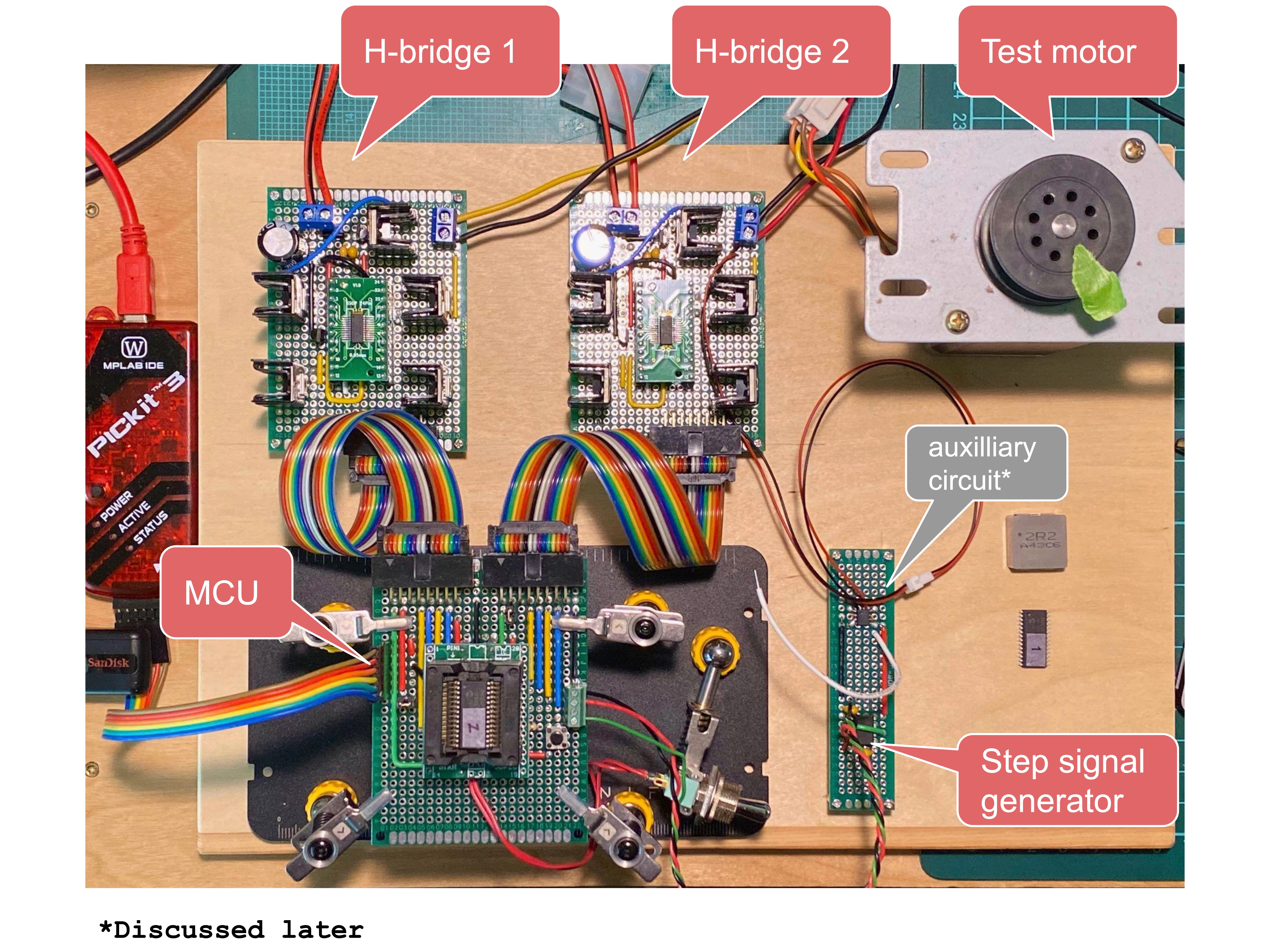
Figure 8: overview per axis
Each H-bridge is composed of 4 high-power N-MOSFETs. The H-bridge driver (located in the center of each H-bridge circuit) is responsible for driving the external MOSFETs as well as measuring current flow through the circuit and detecting error conditions. The MCU is responsible for providing the appropriate step sequence to the H-bridge driver, managing the timing of the step pulses, and responding to current sensing feedback as well as any error conditions.
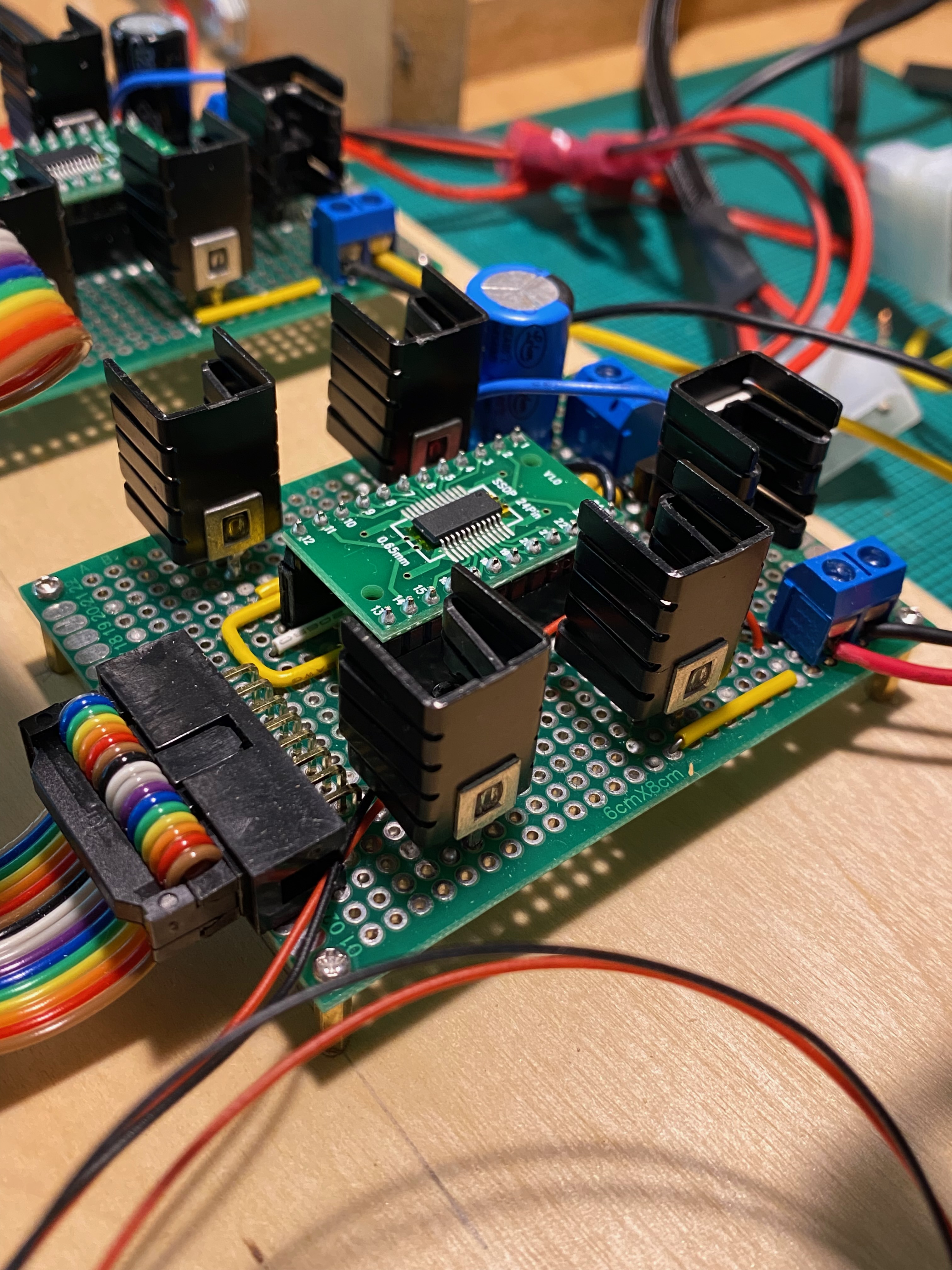
a) H-bridge circuit, iso/top view
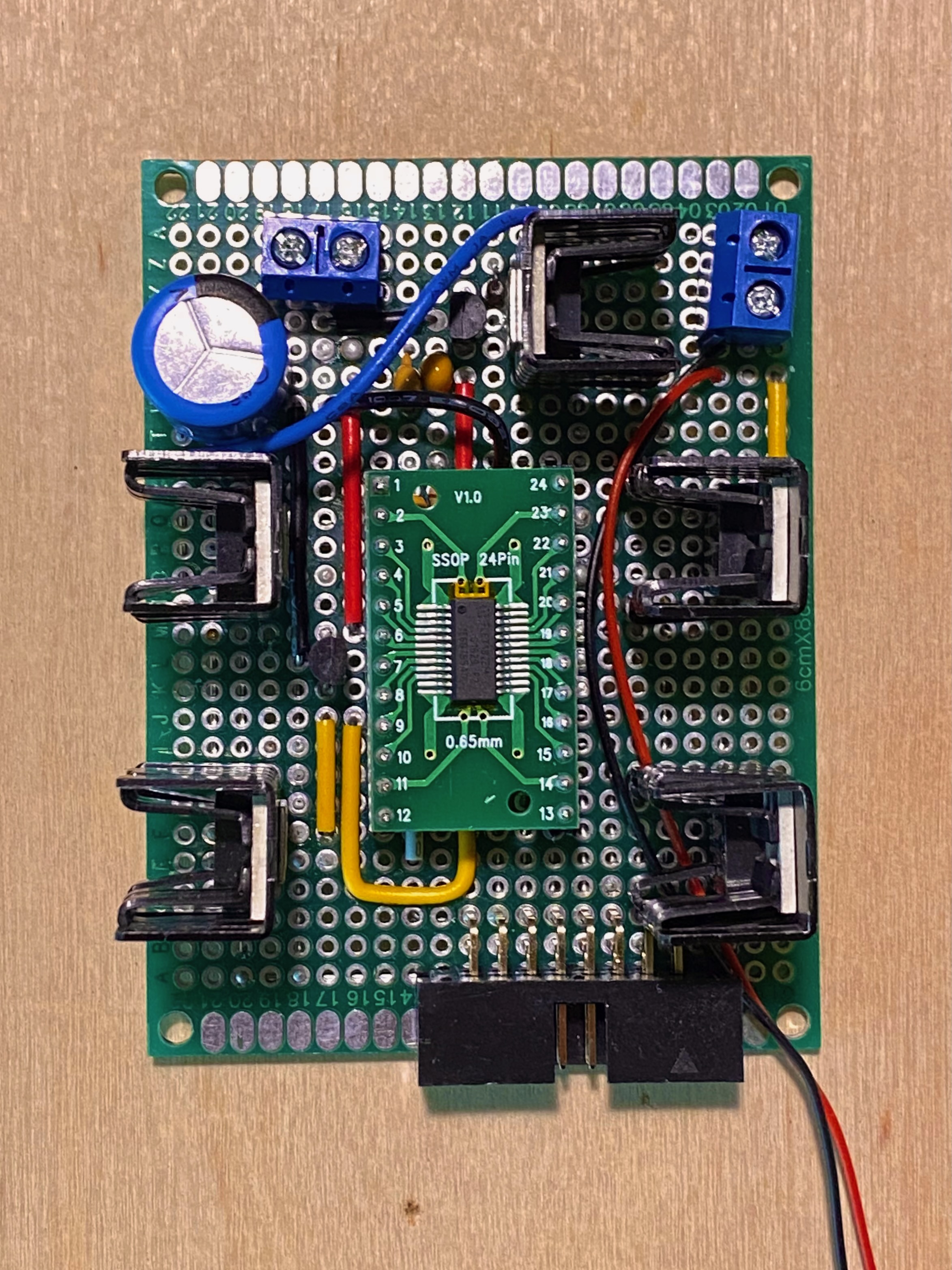
b) H-bridge circuit, top view
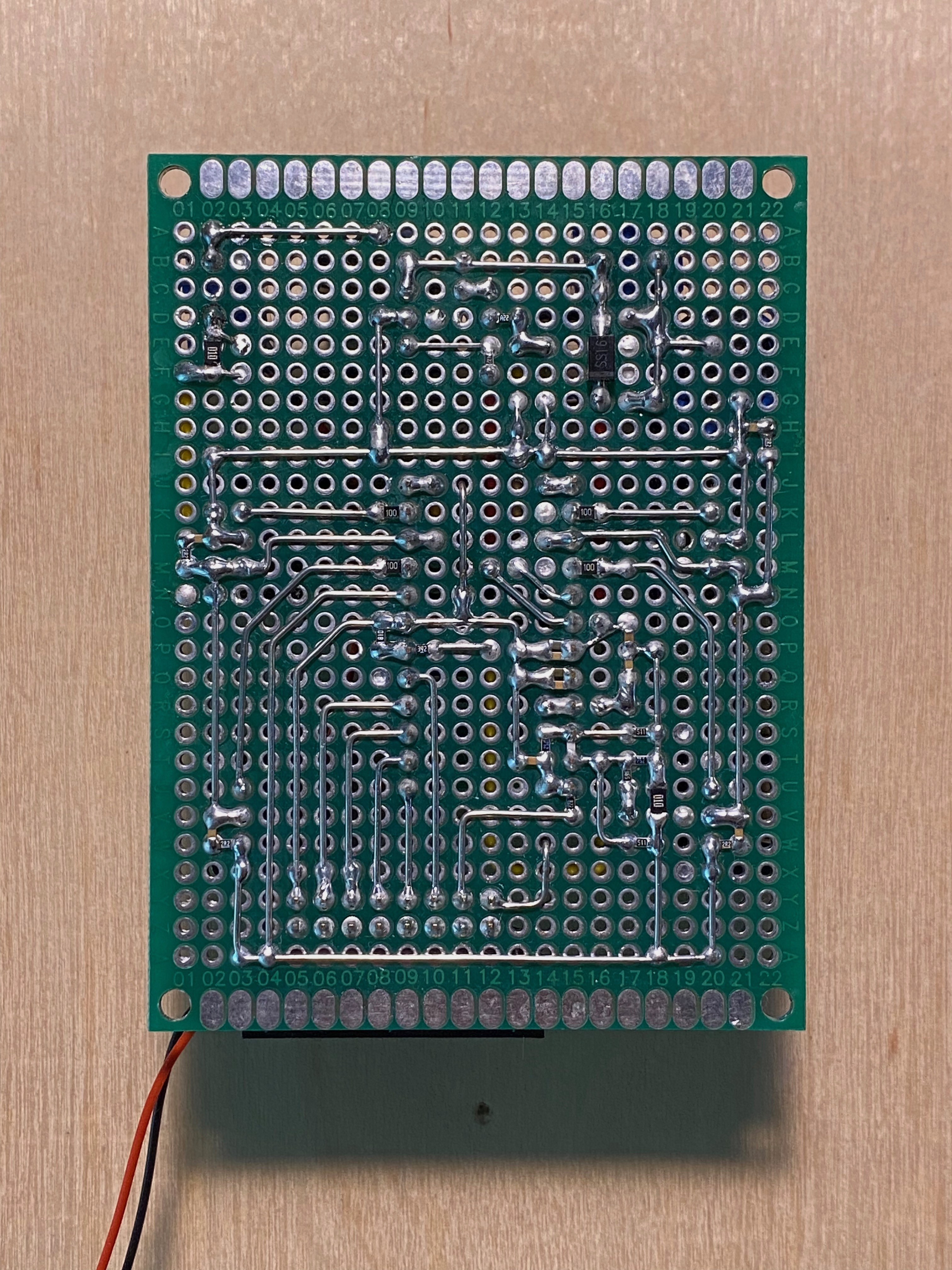
c) H-bridge circuit, bottom view
d) MCU circuit, iso/top view
e) MCU circuit, top view
f) Auxiliary circuit, iso-view
Figure 9: gallery of system sub-circuits
H-bridge + Driver Highlights
The H-bridge circuit was designed with performances highlighted below:
- 0-95% at 20kHz & 100% Duty cycle of High-side MOSFETs
- Protection features: OV/UV, OC, SC, OT, RPP, shoot-thru
- 7.5 ~ 34V operating range
- Each MOSFET capable of up to 110A continuous*
*Refer to appendix on MOSFET selection
H-bridge Driver: Overview
The overall circuit is based on TLE7182EM datasheet recommendation (Figure 10). TLE7182EM from Infineon Technologies was chosen for its convenient set of features, including:
- Independent MOSFET controls
- Integrated analog current-feedback
- Integrated protection features
a) Recommended application diagram
b) H-bridge
c) Reverse-polarity protection
d) Charge pump
e) Low-side current feedback
Figure 10: TLE7182EM: application recommendation [2]
Break-down of driver circuit:
Figure 10b: 4 \(\times \) external MOSFETs per H-bridge with RC turn-off snubber. (Refer to appendix for discussion on MOSFET selection).
Figure 10c: 1 \(\times \) external MOSFET for reverse battery-polarity protection. This is a necessary feature to protect a MOSFET based H-bridge against critical operator error: reverse battery polarity. The controlling element here is an NMOS, which is significantly more power efficient than an in-line diode and more cost effective than a PMOS implementation. The main tradeoff is the complexity of implementation, particularly, an NMOS in this placement requires a charge pump to deliver driving voltages above the rail voltage. TLE7182EM has an integrated charge pump specifically for this. A minor note on the BJT and its accompanying diode: the diode is necessary here to prevent an unplanned avalanche breakdown across the Emitter-Base junction.
Figure 10d: charge pumps reference source voltage of high-side MOSFETs such that the gates of the high-side MOSFETs can be switched robustly.
Figure 10e: integrated op-amp for current feedback.
Using the design recommendation, I designed the following circuit (Figure 11). The physical prototype can be seen in Figure 9b.
Figure 11: actual schematic
There are a few keypoints to take note of regarding the above circuit:
- This circuit has an additional reverse battery polarity protection implemented through diode D2. Through bench testing, it does not seem that TLE7182EM itself is protected against reverse polarity conditions. This added diode contributes to a minor increase to power dissipation and the minimum operating voltage of the circuit, but ensures that the IC is not damaged in the event of reverse battery polarity.
- The RC-snubber is critical to managing MOSFET 'ringing' during turn-off. However, the actual values for them cannot be easily calculated during design, as they depend (in part) on parasitic inductances and capacitances within a physical construction. Therefore, they need to be determined empirically.
- RC filter implement on the analog output of this circuit feeds into the controlling MCU, which may or may not use an ADC to handle the signal. This RC filter in fact might not be necessary if an ADC is not used. This is a topic of later discussion.
At this point, we should also briefly discuss the drive sequence for the external H-bridges. For this initial discussion, we refer to Figure 12.
Figure 12: "slow-decay" drive sequence[3]
Figure 12 illustrates a single winding of a stepper motor being switched ON & OFF. During the “on” phase, the motor winding is first activated by turning on Q1 and Q4. During the “off” phase, the current flowing through the winding is diverted through Q2 and Q4, such that it circulates in the low-side of the H-bridge. This type of drive sequence is called “slow-decay” or “free-wheeling”, as the circulating current in the “off” phase takes on a slow exponential decay, dissipating through the resistances within the winding and low-side switches. The resulting waveforms can be seen on the right side of the image, where the current is shown rising and falling during the “on” and “off” phases. The goal of this switching scheme is to maintain the average current around some target current. In addition, by turning on the two low-side switches during the “off” phase, back EMF from the motor is managed and ripple voltages on the rails are minimized. Using the low-side switches is slightly preferred over the high-side switches for the “off” phase, as the low-side switches do not require charge pumps to operate.
A bipolar stepper motor has a minimum of two sets of windings to achieve sequential steps. In order to actuate the stepper motors used in this project, each motor is controlled by two H-bridges and the order of actuation is ‘staggered’ to achieve sequential steps. In the simplest mode, the motors are activated at “full step”, which is the coarsest but most robust method of driving a stepper motor. Further fractional steps may be achieved by driving the rotor partial way between full steps. In essence, the two windings are actuated at 90° out-of-phase from each other. With further discretization, the drive sequences begin resembling two sine waves, 90°out-of-phase from each other — hence, the name “wave drive”. Figure 13 shows the target currents w.r.t time for the two windings inside the stepper motor.
Figure 13: target winding currents [4]
Basic Implementation: Results
Using the described methods and low-side current sensing, the results of the implemented circuit can be seen below (Figure 14).
Figure 14: { Ch1: Q1 \(\overline{V}_{G}\) Ch2: Low-side \(i_{sense}\) }
Here, channel 1 shows the (inverted) gate signal \(\overline{V}_{G}\) on high-side MOSFET Q1. Overlaid, in channel 2, is the analog measurement output of the low-side sense resistor. We can see that during the “on” phase, the winding current is able to rise until it reaches a pre-set level. Once the current surpasses the pre-set limit, the gate signal is switched, and the system enters the “off” phase, effectively limiting the rising current. An internal clock triggers the “on” phase in the following period, and the cycle repeats.
Figure 15 shows an in-line measurement of the winding current during a wave-drive sequence.
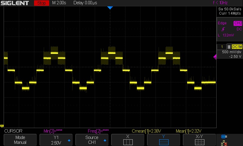
Figure 15: { Ch1: \(I_{motor}\) }
The results from the basic implementation show that the baseline performance is quite good. The waveform shown in Figure 15 exhibits good fidelity, with minimum distortion on the target sinusoidal waveform.
Deep Dive: Current Sensing
In the following sections, I will do a deep dive on the subject of current sensing, as this is a critical part of the working circuit. I will be analyzing the basic implementation and how it can be augmented to yield an improved system.
Low-side Current Sensing
So far the discussion has been focused around low-side current sensing. There are several benefits to using this method of measuring current through the circuit.
In general, low-side current sensing is one of the simplest and most robust methods for measuring current through a system. With the shunt resistor as close to GND as possible, the common-mode voltage on the op-amp inputs are reduced to a minimum (assuming the op-amp is also GND-referenced); the design eliminates the need for specialty op-amps. (Refer to Figure 16 for a detailed view):
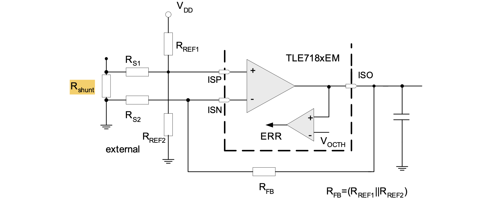
Figure 16: low-side current sensing with TLE7182EM
In addition, since the shunt resistor is placed outside of the H-bridge, current flowing through the system is mapped unidirectionally — regardless of whether the H-bridge is driven in “forward” or “reverse” mode. This simplifies how the analog measurement is handled because 1) unidirectional mapping effectively doubles the resolution of readings when compared with bidirectional readings, and 2) it becomes easy to substitute a comparator circuit in place of an ADC when processing this signal on the MCU side.
Furthermore, the system directly limits the maximum current flowing through the system. This is a valuable feature as the system is capable of drawing very high currents:
\[\frac{V_{s}}{R_{motor}} = I, \; \frac{24V}{0.387\Omega} = 62A\]By design, the components are chosen to handle up to 110A, however, the intention is not necessarily for the current draw to reach this level. The system can achieve good regulation of this current given that \(T_{sys} \) is much faster than the time constant of the load (\(\tau_{motor}\)), and that \(\tau_{motor}\) is much smaller than \(T_{tmr}\) such that current through the load has enough time to decay during its “off” phase.
\[\begin{align} T_{sys} \; &<< \; \tau_{motor} \; << \; T_{tmr} \\ &\small{T_{sys}\text{: instruction cycle of MCU}} \\ &\small{T_{tmr}\text{: PWM period}} \end{align}\]These aspects of low-side sensing come paired with their drawbacks as well. In particular, since current sensing resides outside of the H-bridge, the system is effectively ‘blind’ during the “off” phase:
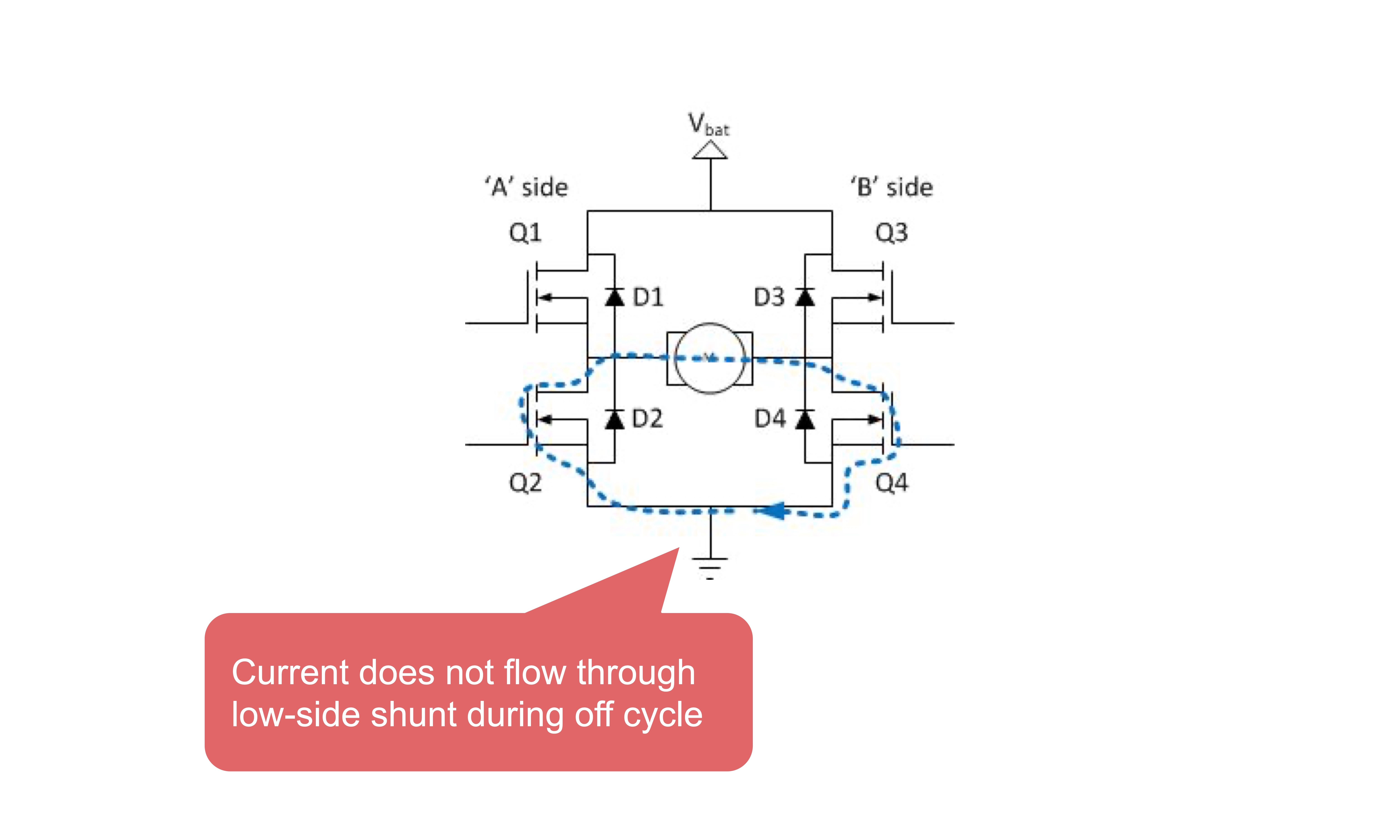
Figure 17: "off" phase
This means that the system does not directly regulate \(I_{motor,avg}\), and that the bridge must be switched into an “on” configuration in order to take measurement of the current through the load. This may lead to distortions on the current waveform; furthermore, it imposes aggressive timing requirements on the switching components and the controlling MCU, specifically how quickly it can handle the analog signal and execute its Interrupt Service Routine (ISR), which is directly related to \(T_{sys}\), the instruction cycle of the MCU. The keypoints for the pros and cons of low-side sensing are highlighted below:
Pros:
- Good bandwidth & accuracy
- Simple implementation:
- does not require special op-amp (at most: rail-to-rail)
- measurement is GND referenced
- unidirectional mapping of current
- Generally good regulation of \(I_{motor} \) for: $$ \begin{align} T_{sys} \; &<< \; \tau_{motor} \; << \; T_{tmr} \\ &\small{T_{sys}\text{: instruction cycle of MCU}} \\ &\small{T_{tmr}\text{: PWM period}} \end{align} $$
- Limits maximum current, \(I_{motor,max}\)
Cons:
- Does not directly regulate \(I_{motor,avg}\)
- System is 'blind' during OFF cycle
- Limiting \(I_{motor,max}\) results in aggressive timing requirements on MCU:
- ISR
- Analog signal measurement
- \(T_{sys}\)
Fortunately, there are some techniques we can employ to substantially improve the timing of the MCU and the overall feedback loop. In terms of the ISR, each ISR should be written as concisely as possible. Depending on the platform for the MCU, it may also be necessary to write the ISR with ASM, as C-language abstraction often causes significant delays in servicing the ISR. To further reduce this delay, \(T_{sys}\) may be boosted via PLL, which is commonly available on PIC microcontrollers.
In terms of timing of the analog signal measurement, I would recommend avoiding ADC’s all together. Typical ADC units on-board of MCUs rely on switched-capacitor circuits, which tend to be noisy and slow. Instead, similar functionality can be achieved through a comparator with a set-point defined by a DAC. The combination of a comparator + DAC relies on a resistor ladder & op-amp — making it significantly faster than an ADC; it also does not impose noise on the measurement! Keypoints listed below:
Improving timing:
- Write short, concise ISR
- Write ASM — C Language abstraction causes large delays
- Increase \(T_{sys}\) → PLL
- reduces delay between interrupt occurence and ISR execution
- Choose {DAC + comparator} vs. ADC
- Switched cap. ADC: slow, noisy
- {DAC + comparator}: resistor ladder + OpAmp — fast, does not introduce noise on measurement
The final drawback in low-side sensing is the topic of current distortion when driving an inductive load under a wave-drive scheme:
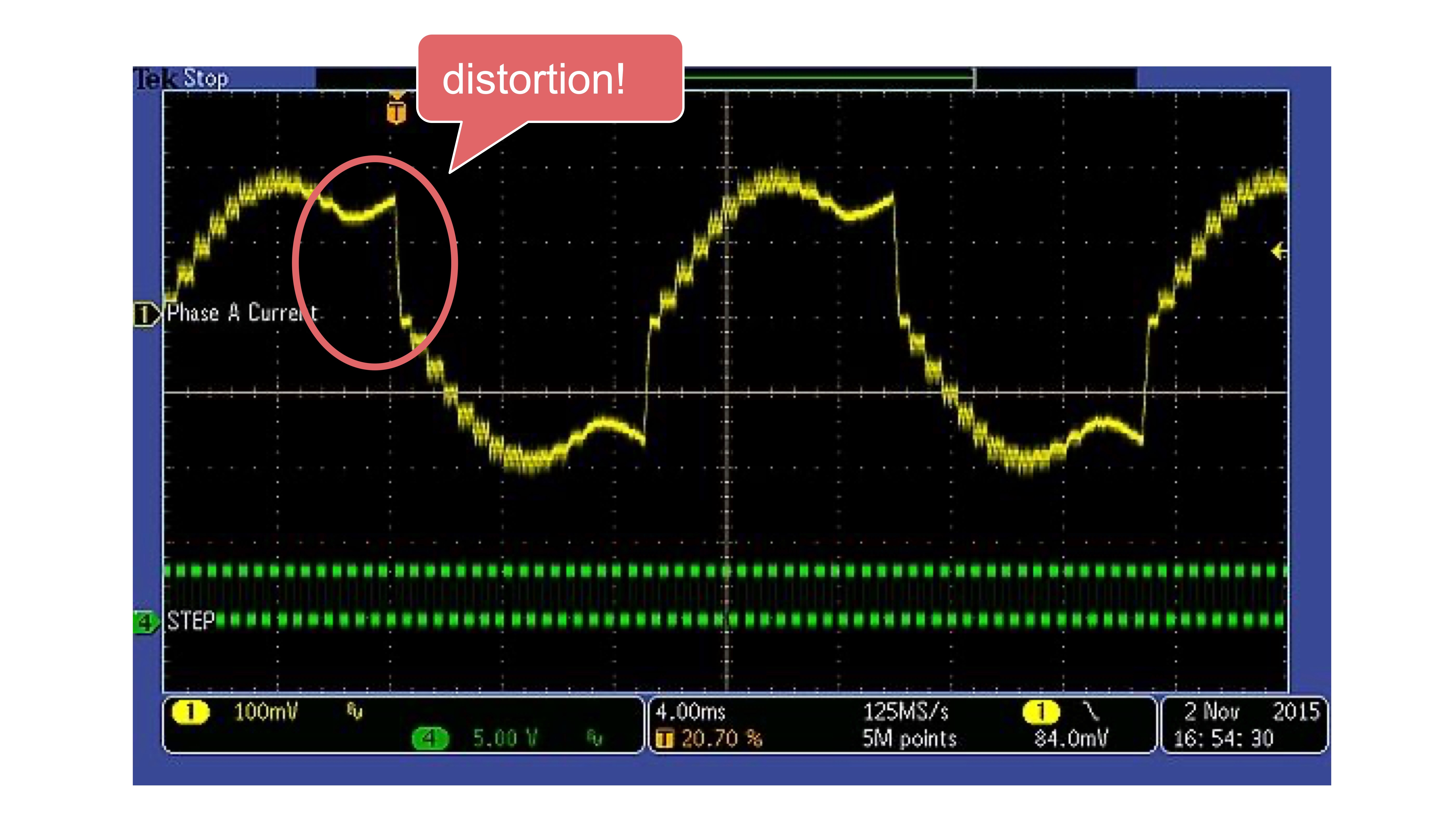
Figure 18: current distortion (slow decay)[5]
Notice that distortion occurs when the current is expected to move towards 0. A combination of factors contribute to this distortion, with the primary reason being that the H-bridge must be turned ON to measure the state of \(I_{motor}\). During this brief “on” period, the current through the system is rising even though the overall control may be attempting to control it towards zero. Other key factors are summarized below:
Current Distortion (slow decay)
- System being 'blind' during OFF cycle
- Must turn ON H-bridge to measure state of \(I_{motor}\)
- Inadequate timing
- Only using Slow Decay
- Other modes may be unsafe without full visibility of \(I_{motor}\)
Distortion may be improved with faster timing, however, it is almost unavoidable when running only the basic implementation discussed so far…
Improvement: In-line current sensing!
We can improve upon the basic implementation by using “in-line” current sensing. Figure 19 illustrates this concept.
Figure 19: shunt resistor placement in "in-line" current sensing[3]
The first benefit of having a sense resistor in this placement is pretty obvious: the system has visibility of the magnitude and direction of \(I_{motor}\) at all times. This information is crucial in effectively driving the load towards 0 in the wave-drive scheme. In the the previous approach (i.e. low-side sensing), the system is limited to the natural decay of current “free-wheeling” through the motor — a relatively slow process — hence the name “slow-decay”. The method of “slow-decay” produces distorted sine waves when the natural decay rate of the load is slower than the decay rate of the target trajectory (sine wave).
The problem is further exacerbated when the H-bridge is briefly turned ON to measure to current flow at each start of cycle — effectively increasing the current through the load before allowing it to decay.
By having an in-line shunt resistor to the load, it is no longer required for the H-bridge to switch ON for the system to measure current flowing through the load. In addition, with information on the direction flow of current, the system is now allowed to utilize “fast-decay” to drive current flow in the reverse direction during the “off” phase (see Figure 20). This significantly improves the response time of the system when driving the load towards 0, minimizing distortion to the target trajectory. Figure 21 shows how “fast-decay” is used to quickly decrease the motor current to match the (decreasing) target current.
Figure 20: "fast-decay" control scheme[3]
Using in-line sensing, the system now also has the option to directly regulate the average current through the motor winding \(I_{motor,avg}\) as opposed to only limiting the peak current \(I_{motor,max}\) (as in the case of low-side sensing). This reduces dependency on aggressive timing of the switching components. Having a robust H-bridge that can handle large currents also helps us further capitalize on this. Depending on the application, if a load is not sensitive to larger ripple currents and instead prioritizes average current, in-line current sensing enables looser timing while still maintaining a controlled \(I_{avg} \).
Figure 21: fast-decay utilization when decreasing target current ( − − red dotted line)[5]
Figure 22: fast-decay effects on overall wave-drive accuracy[5]
I designed a basic implementation of an in-line sensing circuit; the schematic is shown in Figure 23. This implementation relies on the specialty op-amp LMP8601MA from Texas Instruments, which features a precision-trimmed resistor network, high CMRR, and high tolerance to common mode voltages (CMVR).
Figure 23: LMP8601MA in-line current sensing circuit
Circuits measuring voltage across an in-line shunt resistor are generally more complex than their low-side counterpart. Because voltages on either ends of the shunt resistor are now floating at some voltage high above common GND, circuits that are GND-referenced need to filter out the common mode voltage, demanding high CMRR, CMVR, and a well balanced resistor network to reduce errors in measurement. Furthermore, as the expected output is now bi-directional, the analog-to-digital conversion range needs to be allocated for both positive and negative swings — effectively halving the resolution w.r.t. the unidirectional version. To center the zero voltage in a full ADC range further requires a well tuned virtual-GND. Luckily, specialty op-amps like LMP8601MA and similar op-amps labeled as “current-sensing op-amps” with rail-to-rail capabilities can take on most of these design challenges.
Figure 24 shows the placement of this auxiliary circuit on the bench testing platform.
Figure 24: location of auxiliary circuit
A summary of the benefits and drawbacks of the in-line current sensing method:
Pros:
- Bi-directional current sensing
- Direct measurement of \(I_{motor}\) at all times
- not reliant on state of H-bridge
- less noisy
- enables other driving modes (e.g. "fast-decay")
- less current distortion
- System may prioritize regulating \(I_{motor,avg}\)
- reduces dependency on aggressive timing of switching components
Cons:
- More complex design
- 'Requires' specialty OpAmp:
- high CMRR/CMVR: inputs are floating at voltages above GND
- precision-trimmed feedback network
- rail-to-rail capability
- precision virtual GND
- Bi-directional output leads to reduced resolution on ADC range
… more
References
- STMicroelectronics, “Stepper-Motor Performance Constant-Current Chopper Driver UPS”, AN468 Application Note, December 2003.
- Infineon Technologies AG, "TLE7182EM H-Bridge and Dual Half Bridge Driver IC", Rev 1.1, September 2010.
- Modular Circuits, http://modularcircuits.tantosonline.com/blog/articles/h-bridge-secrets/sign-magnitude-drive/
- Monolithic Power Systems, "MP6500 35V, 2.5A, Stepper Motor Driver", Rev 1.0, June 2017.
- eeNews Europe, “Improving current control for Better Stepper Motor Motion Quality,”, https://www.eenewseurope.com/en/improving-current-control-for-better-stepper-motor-motion-quality/, February 2016.